Rainbow-electronics AT27C4096 User Manual
Browse online or download User Manual for Storage Rainbow-electronics AT27C4096. Rainbow Electronics AT27C4096 User Manual
- Page / 12
- Table of contents
- BOOKMARKS
- 4-Megabit 1
- (256K x 16) 1
- OTP EPROM 1
- AT27C4096 1
- 0311F–10/98/xM 12
Summary of Contents
1Features•Fast Read Access Time - 55 ns•Low Power CMOS Operation– 100 µA Maximum Standby– 40 mA Maximum Active at 5 MHz•JEDEC Standard Packages– 40-Le
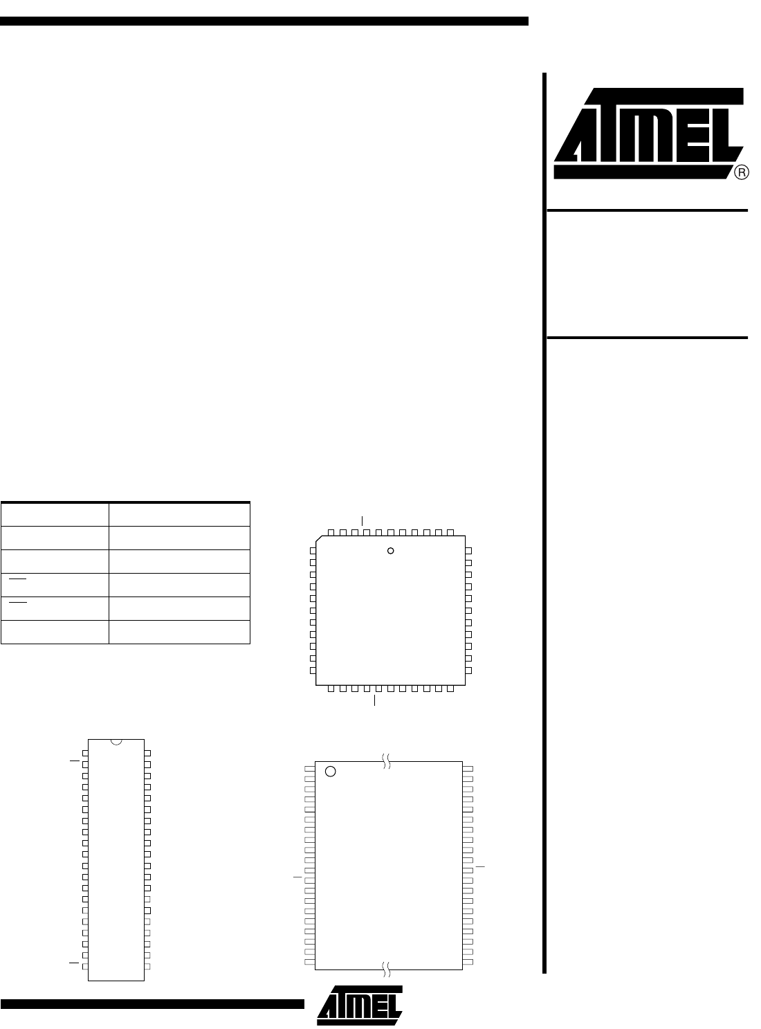
AT27C409610Packaging Information.045(1.14) X 45°PIN NO. 1IDENTIFY.045(1.14) X 30° - 45°.012(.305).008(.203).021(.533).013(.330).630(16.0).590(15.0).04
AT27C409611
© Atmel Corporation 1998.Atmel Corporation makes no warranty for the use of its products, other than those expressly contained in the Company’s standa
AT27C40962less than 55 ns, eliminating the need for speed-reducingWAIT states. The by-16 organization makes this part idealfor high-performance 16- an
AT27C40963Note: 1. Maximum voltage is -0.6V dc which may undershoot to -2.0V for pulses of less than 20 ns. Maximum output pin voltage is VCC + 0.75V
AT27C40964Notes: 1. VCC must be applied simultaneously or before VPP, and removed simultaneously or after VPP.2. VPP may be connected directly to VCC,
AT27C40965AC Waveforms for Read Operation(1)Notes: 1. Timing measurement references are 0.8V and 2.0V. Input AC drive levels are 0.45V and 2.4V, unles
AT27C40966Programming Waveforms(1)Notes: 1. The Input Timing Reference is 0.8V for VIL and 2.0V for VIH.2. tOE and tDFP are characteristics of the dev
AT27C40967Notes: 1. VCC must be applied simultaneously or before VPP and removed simultaneously or after VPP.2. This parameter is only sampled and is
AT27C40968Rapid Programming AlgorithmA 50 µs CE pulse width is used to program. The address isset to the first location. VCC is raised to 6.5V and VPP
AT27C40969Ordering InformationtACC (ns)ICC (mA)Ordering Code Package Operation RangeActive Standby55 40 0.1 AT27C4096-55JCAT27C4096-55PCAT27C4096-55VC
Related products and manuals for Storage Rainbow-electronics AT27C4096
 (41 pages)
© 2020, manymanuals.com. All rights reserved. | 0.625 s |
 Manymanuals.com
 Manymanuals.de
 Manymanuals.fr
 Manymanuals.it
 Manymanuals.pl
 Manymanuals.cz
 Manymanuals.es
 Manymanuals-pt.com
Comments to this Manuals